
JFET or Junction Field Transistor is the field effect transistor to be developed that can be used as a voltage controlled resistance or as an electronically controlled switch.
In this, we are going to explain you The working operation of Jfet and biasing in detail.
Recommended Reads Before Going Forward:
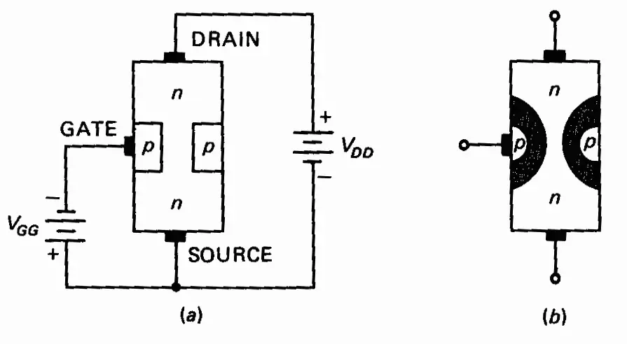
Junction Field Effect Transistor Construction
JFET consist of the channel of semiconducting material through which current flows. Jfet are of two types; one is n-channel JFET and another is p-channel JFET.
Generally, n-channel JFET are more preferred than p-channel JFET because in n-channel electrons are the majority carriers and as we know electrons are more mobile than holes.

In an N-channel JFET, two smaller pieces of p-type silicon material diffused on the opposite sides of its middle part forming p- n junction and an n-type silicon bar considered as the channel.
Similarly in p-channel JFET, smaller pieces of n-type silicon material diffused on the opposite sides of its middle part forming p- n junction and a p-type silicon bar considered as the channel. The p-n junction forms a terminal or gates internally known as a gate terminal.
By using battery it makes ohmic contacts at the two ends of the channel; one is called source terminal and other is called Drain terminal. Gate terminal is used to control the flow of current from source to Drain. Gate-source forms one p-n junction diode while Drain forms another p-n junction diode. These diodes are known as the gate -source diode and gate- drain diode.
JFET Working Operation
Both N-channel JFET and p-channel JFET are operated in the same way, although the charge carriers are inverted i.e. electrons are majority carriers in n-channel and holes are majority carriers in p-channel. Here we explain n-channel jfet operation because it is more preferable.
The width of the channel varies in accordance with the magnitude of the bias applied to the gate terminal and source-drain terminal. As shown in the figure above we explain how channel width change when we apply either a positive voltage or negative across it. Let’s have a detailed look at it.
Jfet operates in three conditions depending upon the voltage applied across terminals:
(i) No voltage:
When neither any voltage is applied across source to drain terminal i.e. Vds = 0 nor any bias is applied to the gate terminal i.e. Vgs= 0, the depletion region around the p-n junction are of equal thickness and symmetrical in nature.
(ii) Negative Voltage:
When the gate is negative bias with respect to the source and drain is applied with a positive bias with respect to the source, the p-n junction got reverse biased and forms depletion region. When the drain current flows through the channel, there is a voltage drop along its length.
The result is that the reverse bias at the drain end is more than that at the source end making the width of depletion layer more at the drain. With the increasing resistance and reducing current Id , the channel starts narrowing.
If we further increase the negative voltage across the gate, depletion layers meet at the center and the drain current cut off completely.
Similarly, if we reduce the negative voltage across the gate, the depletion layers start reducing causing decrease in resistance and increase in drain current Id.
(iii) Positive voltage:
When a positive voltage is applied to the drain terminal with respect to source terminal without connecting the gate terminal to the supply, the electrons starts moving from source terminal to drain terminal whereas conventional drain current Id flows through the channel from Drain to the source.
Due to this flow of current, the uniform voltage drop occurs across the channel resistance which reverse bias the diode. The gate is more negative to those points in the channel which are nearer to drain than the source.
Therefore, depletion layers penetrate more deeply into the channel at points which are more closer to drain than the source. As a result, the wedge-shaped depletion regions are formed when Vds is applied across the terminals.
Characteristics of JFET
The characteristic curve indicates the behavior of the device by increasing or decreasing current and voltages applied across their terminals. There are two types of static characteristics of JFET:
(i) Output or Drain characteristics:
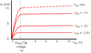
The curve drawn between drain current Id and drain-source voltage VDS along y-axis and x-axis with gate to source voltage Vgs as the parameter is called the drain or output characteristic. As shown in the figure below, the curves are very nearly horizontal at voltages greater than the pinch-off voltage.
(ii) Transfer characteristics:
By keeping the drain-source voltage constant VDS and finding the drain current Id for various values of gate-source voltage Vgs ,the transfer characteristics can be determined experimentally.
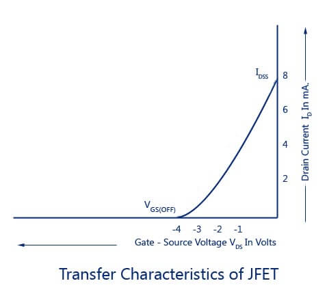
As shown in the figure above, we observe the following things from its curves are:
- When Vgs = 0 then Drain current Id = Idss
- When Vgs = Vd then Drain current Id = 0
- Drain current decreases with an increase in negative gate-source bias.
Applications of Junction Field Effect Transistor JFET
Junction Field effect transistor is widely used in various applications because of its extraordinary features. Following are:
- Voltage-controlled Resistor
- Differential Amplifier
- Constant current source
- Low noise Amplifier
- High input impedance Amplifier
- Analog Switch or gate
Before you go…
Junction Field Effect Transistors or JFETs is a very vast topic and there are different types of Field Effect Transistors. Here we are sharing some more guides related to transistors that will enhance your knowledge. We hope you will enjoy reading them too.
This information is so clear and straight forward.Thanks….
Valuable knowlege about jfet
Now I am clear with JFET ,thanks
Your welcome Vivek. I am happy that we are of any help to you in your study. For more tutorials, like our facebook page 🙂