
Fet is categorized into Jfet and Mosfet, both are quite similar in their operating principles and electrical properties. In our previous articles, we explain Fet transistors and its operation, pn junction diode characteristics in detail. Here we are going to explain you in detail about JFET , Mosfet and difference between them.
JFET( Junction Field Effect Transistor)
JFET is a voltage controlled semiconductor device used as amplifiers, electronically controlled switches and voltage controlled resistors in many applications. Junction field effect transistor has no p-n junctions but has a high resistivity semiconductor material forming a channel of either n-type or p-type silicon for the majority carriers to flow through with two ohmic electrical connections at either end commonly known as Drain and source.
(i) Jfet Configuration:
Two basic configurations of Junction field Effect Transistor are:
(i) N-channel Jfet: In n channel jfet’s, channel is generally doped with donor impurities i.e., into this the flow of current through the channel is negative in the form of electrons.
(ii) P-channel Jfet: In p channel jfet’s, the channel is generally doped with acceptor impurities i.e., into this the flow of current through the channel is positive in the form of Holes.
Note: N-Channel Jfet’s have a greater channel conductivity than P-channel JFET’s because electrons have a higher mobility through a conductor compared to holes.
(ii) Jfet construction and symbols:
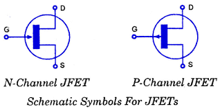
In N-channel jfet, we basically diffuse two smaller pieces of p-type material on either sides of the middle part while in P-channel Jfet we diffuse two smaller pieces of n-type material on either side of the middle part, forming p-n junction. The two p-n junctions forming diodes or gates are connected internally and a common terminal called the gate terminal is brought out. At the two ends of the channel, two ohmic electrical connections are made; one lead is called the source terminal and other is called the drain terminal denoted as S and D.

Schematic symbols of n channel and p channel is shown above. The vertical line in the symbol may be thought of channel and source and a drain connected to the line. When the gate junction is forward biased, the direction of the arrow at the gate side indicates the direction in which the gate current flows. In n-channel and p-channel JFET, the arrow at the junction points inside and outside the device respectively.
Mosfet( Metal Oxide Field Effect Transistor)
Mosfet is a voltage controlled field effect transistor has a metal oxide gate electrode that is electrically insulated from the n-channel or p-channel by a very thin layer of insulating material usually silicon dioxide commonly known as glass. For integrated circuit technology where power limitation is a major concern, Mosfet’s played a vital role because they offer very high input impedance.

(i) Mosfet configurations:
Two basic configurations of Metal-oxide Field-effect transistor are:
(i) Enhancement Mode Mosfet: These devices are off at zero gate-source voltage and can be turned on by pulling the gate voltage on either higher than the source voltage, for NMOS, or lower than the source voltage for PMOS.
(ii) Depletion mode Mosfet: These devices are off at zero gate-source voltage. For n-type device, the threshold voltage might be about -3V, so that it could be switch on by pressing the gate 3V negative while for p-type the polarities are reversed.
(ii) Mosfet symbols and construction:
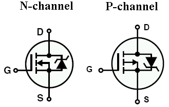
The basic symbols and its construction of Mosfet’s are shown below.
Mosfet transistor consists of four terminals; source, drain, gate and substrate. Gate of this transistor is insulated from the semiconductor by a layer of Sio2 or another dielectric. The Source is the terminal through which the majority carriers enter the channel and drain are the terminal through which majority carriers leave the device. The fourth additional terminal known as the substrate is not normally used as either an input or output connection but instead it is used for grounding the substrate.
In enhancement type MOSFET the application of a gate voltage activates the channel by inducing a layer of carriers between source and drain. In depletion type mosfet, the gate voltage can either reduce or increase the channel current.
Difference between JFET and Mosfet:
Jfet and Mosfet are two types of Field effect transistors, similar in various aspects. In the table given below, we explain how it differs from each other.
[su_table responsive=”yes”]
| JFET | Mosfet |
| JFET Operates only in depletion mode | Mosfet operates in both Enhancement and Depletion mode |
| Reverse biasing of the gate terminal controls the Conductivity | Carriers induced in the channel controls the Conductivity |
| JFET has High Gate current | Mosfet has low Gate current |
| JFET Input Impedance is High | Mosfet Input Impedance is Very High |
| Characteristics curve is Flatter | Less Flat characteristics curve in comparison to JFET |
| Drain Resistance of JFET is High | Drain Resistance is Low |
| Manufacturing Process is Simple | Mosfet has Difficult manufacturing process |
| It is a 3 terminal device | Mosfet has 4 terminals |
[/su_table]
Hope you all like this article. For any suggestions please comment below. We always appreciate your suggestions.