

Great magic done by the Ashutosh Tiwari and his team, have discovered first stable p-type 2D semiconductor material at the University of Utah that opens the door for much speedier smartphones and computers. The semiconductor made of the element tin and oxygen, tin monoxide ( SnO) is a layer of 2D material only one atom thick, allows electrical charges like electrons to move through it at a faster speed than conventional 3D material such as silicon, germanium etc.
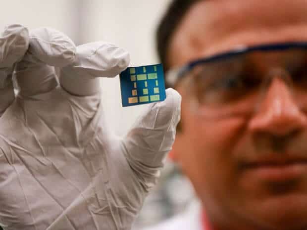
[Photo:Dan Hixson/University of Utah College of Engineering]
Researchers in the field of engineering materials have discovered that new types of 2D material such as graphene, molybdenum disulfide and borofene etc allow only the movement of N-type or negative electrons. In order to create an electronic device, however, you need semiconductor material which allows the movement of both negative electrons and positive charges known as holes. By the discovery of tin oxide material, Ashutosh Tiwari proved that 2D material is the new ray of hope for smaller, faster and lower power transistors.
In future, if we diffuse this p-type 2D semiconductor with n-type 2D semiconductor in a transistor, it opens up the possibility of building power saving two-dimensional complementary logic circuits like the ones in the microprocessors today. This material could be the life blood of all electronic devices such as graphic processors and computer processors in desktop computers and mobile devices.
A paper describing the research was published online in the journal, Advanced Electronic Materials on Monday, February 15.
The paper, which also will be the cover story in the printed version of the journal, was co-authored by University of Utah materials science and engineering doctoral students K. J. Saji and Kun Tian, and Michael Snure of the Wright-Patterson Air Force Research Lab near Dayton, Ohio.
The aim of this discovery is to make devices 100 times faster than a regular device i.e. transistors can become even smaller meaning more can be packed on a single chip for more powerful processors because computer processors comprise of billion of the transistor. 3D materials such as silicon consist of multiple layers on a glass substrate allow electrons to bounce around all layers in all directions while 2D material allows electrons to move in one atomic layer in one direction shows faster electron transport.
Ashutosh Tiwari says that by using 2D material there will be less friction meaning the processor will not get as hot as normal computer chips. They also will require much less power to run, a boon for mobile electronics that have to run on battery power. Even this could be especially important for medical devices such as electronic implants that will run longer on a single battery charge.