
Every student faces difficulty understanding the concept of Tunneling effect in the tunnel diode. Students are much confused about different types of diodes they encounter in their academics. We have already explained Photodiodes, Zener diode, Schottky Diode, LED etc. Now, we are going to explain about Tunnel diode, working operation, construction, and applications etc.
What is a Tunnel Diode?
A Tunnel diode is a p-n junction device which exhibits negative resistance. With Negative resistance, we mean “By Increasing the voltage the current through it decreased“. It is also known as Esaki diodes named after Leo Esaki. He received the Nobel Prize in 1973 for the discovery of electron tunneling effect.
In part of their operating range, these diodes have negative differential resistance and therefore are used in frequency converters, detectors, oscillators, amplifiers, switching circuits using hysteresis etc.
Tunnel Diode:
Tunnel Diode construction:
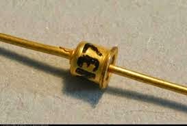
It is a two terminal device with p-type semiconductor acts as an anode and n-type semiconductor acts as a cathode. These diodes are usually fabricated from germanium, gallium arsenide and gallium antimonide. As compared to the ordinary diode, this diode has 1000 times higher doping density.
Because of its heavy doping feature, it reduces the reverse breakdown voltage to a very small value, reduces the width of the depletion layer and produces a negative resistance section on the VI characteristics of the diode.
Important to Note:
Silicon is not used for its construction because the ratio of the peak value of forward current to valley current is small of the order of 3.
Equivalent circuit:
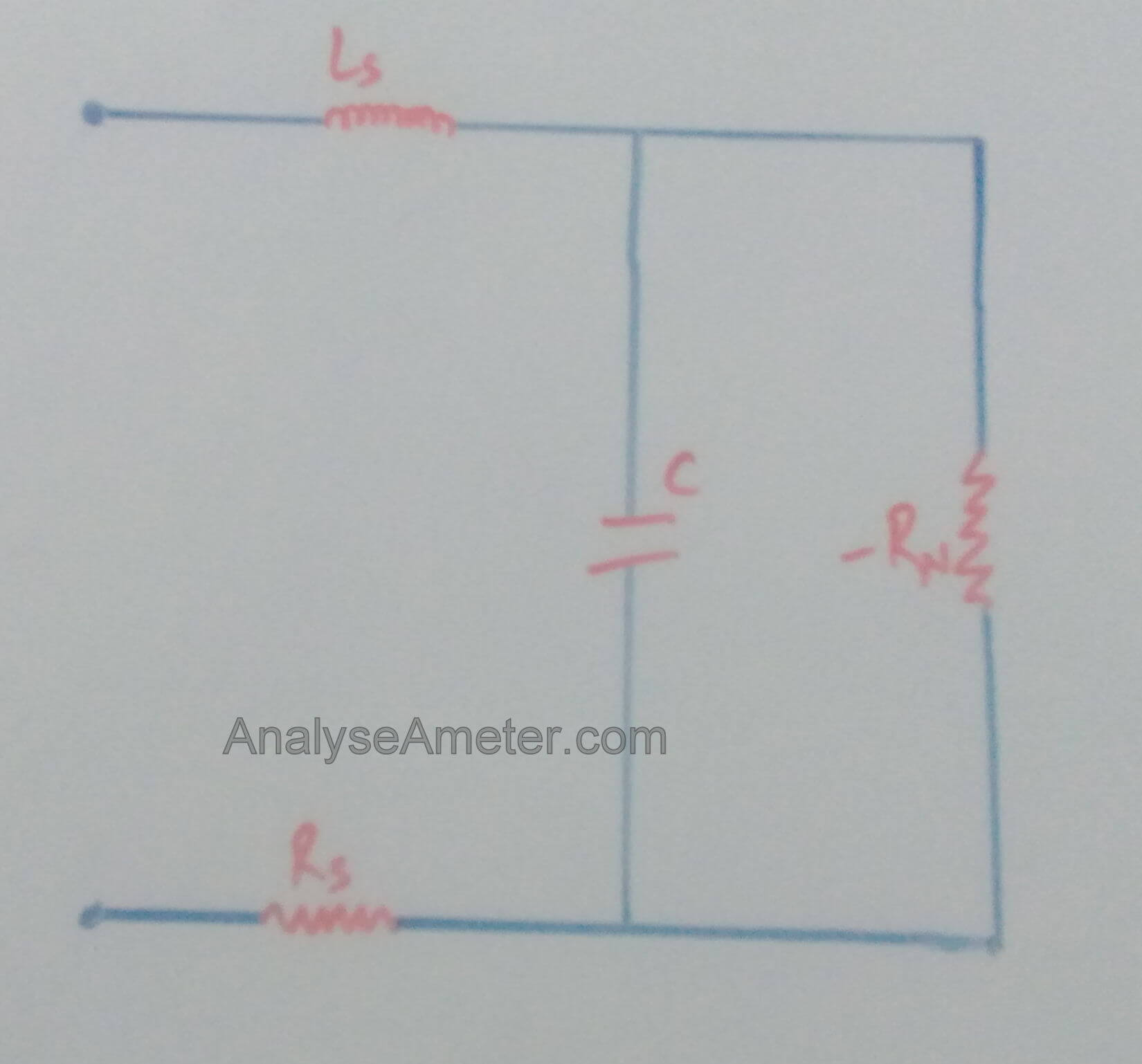
The equivalent circuit of tunnel diode is shown above. The inductor Ls is due to the terminal leads (0.1 to 4nH) and resistance Rs is due to the ohmic contacts, leads and semiconductor materials (1 to 5 ohms). The capacitance C is the junction diffusion capacitance (1 to 10 pF) is connected in parallel to the negative resistance (-RN). These factors play a vital role in determining the switching speed limit and also limit the frequency at which the diode is used.
Tunnel diode Working principle:
The working principle of tunnel diode is based on tunnelling effect. According to laws of physics, the charged particle can cross the barrier only if its energy is equal to the energy barrier. If the energy of the charged particles is less than the barrier energy then they will not cross the barrier. Tunnelling is a quantum mechanical effect which would be impossible according to the mechanics. This effect allows the particle to cross the barrier with less energy than the barrier energy. As per equation, the probability increases with a decrease in the barrier energy.
P α exp (-A*Eb *W)
Where
p = probability
Eb = barrier energy
W = Barrier width
Tunnel Diode operation:
Tunnel diode can operate either in a forward direction or reverse direction. Here we are explaining the operation of the tunnel diode in both biasing. Operation with the help of V-I characteristics curve is explained in the next heading below.
Forward biasing:
In forward bias operation, when the voltage increases electrons at the first tunnel start to flow through the narrow p-n junction barrier and got aligned with empty valence band holes on the p-side of the p-n junction. As voltage increases, this state becomes misaligned and, as a result, the current starts falling. The region into which the current drops is known as negative resistance region. By increasing voltage further, diode begins to operate as a normal diode into which electrons starts moving across the p-n junction through conduction and no longer by tunneling through the p-n junction barrier.
Reverse Biasing:
In Reverse bias operation, filled state on the p-side of the junction becomes increasingly aligned with empty states at the N-side. When they get properly aligned electrons starts tunnel through the p-n junction barrier in the reverse direction. In the reverse direction, these are also known as back diodes and can act as fast rectifiers with extreme linearity for power signals and zero offset voltage.
Tunnel Diode characteristics:
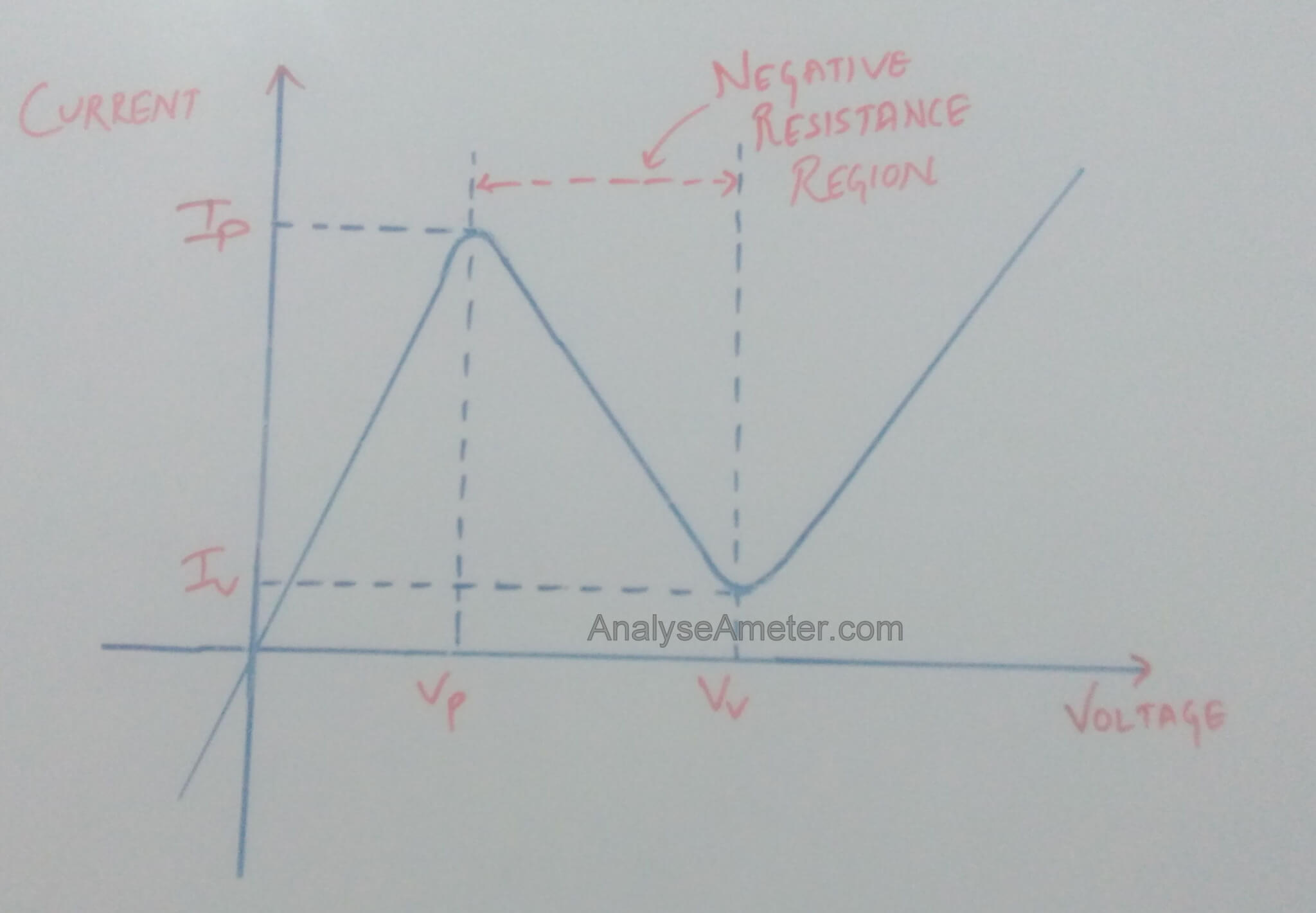
As shown in above figure, the characteristic curve of tunnel diode shows an area of negative resistance. When we forward bias the diode, current quickly rises to its peak value Ip when the voltage reaches its peak value Vp at point A. When we increase forward voltage further, diode current starts decreasing till it reaches the minimum value called the valley current (Iv) and corresponding to valley voltage Vv at point B. For voltage greater than Vv, current again starts increasing further. Between the point A and B, tunnel diode exhibits negative resistance because in this region current decreases with increase in voltage. This is the important property of Tunnel diode because instead of absorbing power, a negative resistance produces power. Negative resistance permits oscillations in oscillator by offering losses in L and C components of the tank circuit. Hence, that’s why it is used as a very high-frequency oscillator.
Note: From Point A to B, current decreases as voltage increases which further increases the negative resistance of the diode.
Applications of Tunnel Diode:
A Tunnel diode is a special kind of diode commonly used for following purposes. Following are its applications:
- Due to a triple valued feature of its current curve, it is used as a logic memory storage device.
- Due to small capacitance, inductance and negative resistance it is used in relaxation oscillators and microwave oscillators.
- Due to tunnelling mechanism, it is used as an Ultra high switching speed because it has a switching time of the order of nanoseconds or even picoseconds.
- It is also used as an amplifier and mixers.
Advantages and Disadvantages of Tunnel Diode:
Each and every diode has its own pros and cons depending on its features. The advantages and disadvantages of this diode are given below.
Advantages:
- Environmental immunity
- Low power dissipation
- High speed of operation
- Low noise
- Longevity
- Simplicity in fabrication
- Ease of operation
- Insensitivity to nuclear radiation
Disadvantages:
- There is no isolation between input and output circuit because it is a two-terminal device.
- Low output voltage swing.
Hope you all like this article. Rate the article below. For any suggestions please comment below. We always appreciate your suggestions.
please sir, explain more on electronics for me please
Hello Sekinat,
Thanks for dropping your comment here. I will be pleased to help you. Just tell us in the comment on what topic do you want our help and we will update the topic here for all.
Nice job sir
Thanks Vivek,
If you have any question regarding electronics, you can ask it here. 🙂