Schottky diode is also known as the hot carrier diode is made up of semiconductor-metal junction rather than a p-n semiconductor junction. It is widely used for radio frequency, RF applications as a mixer or detector diode. In our previous articles, we explain about Zener Diode, Light emitting diode, Photodiode etc. In this article, we are going to explain Schottky diode operation, construction and factors etc in detail.
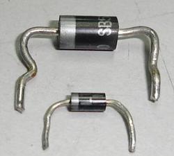
It was named after German Physicist Walter H. Schottky, the barrier means the potential energy barrier for the electrons at the junction. This diode has a low forward voltage drop usually between 0.15 and 0.45 volts and a very fast switching speed. Due to this property, it is also used as power applications as a rectifier.
Schottky diodes:
Schottky diode construction:
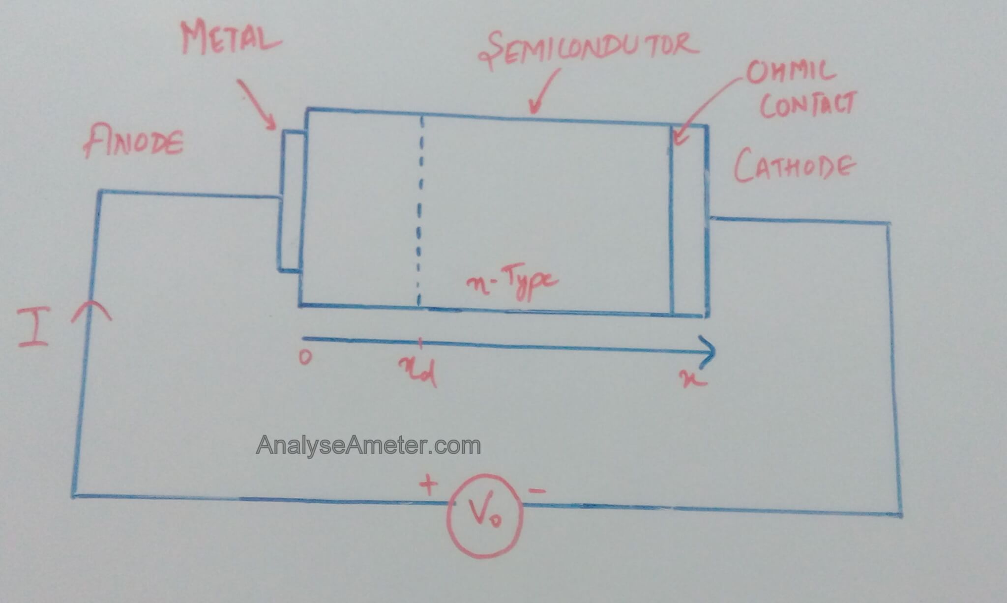
In this diode, junction formed between metal and semiconductor creates Schottky barrier i.e. metal side acts as an anode and n-type semiconductor acts as a cathode. The choice of the combination of the metal and semiconductor determines the forward voltage of the diode. Both n-type and p-type semiconductor can develop Schottky barriers but p-type semiconductor has a much lower forward voltage compare to the n-type semiconductor. As we know, a forward voltage is inversely proportional to leakage current i.e. if the forward voltage is low than the reverse leakage current us high which is not preferable. That’s why we are using n-type semiconductor material in this diode. Typical metals used in the construction of Schottky barrier diode are platinum, chromium or tungsten, palladium silicide, molybdenum, platinum silicide, gold etc.
Schottky diode symbol:
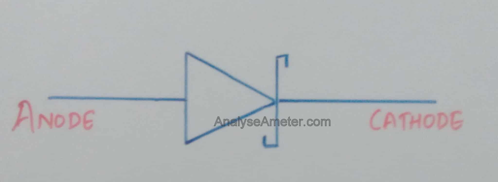
As shown in circuit diagram above, it is a two terminal device; anode and cathode. Metal side acts an anode and n-type semiconductor side acts as a cathode. The circuit symbol is just like a triangle butting up against a line i.e. the terminal entering at the flat edge of the triangle represents the anode. For protection purpose, metal layer is surrounded by gold or silver layer.
Schottky diode Working:
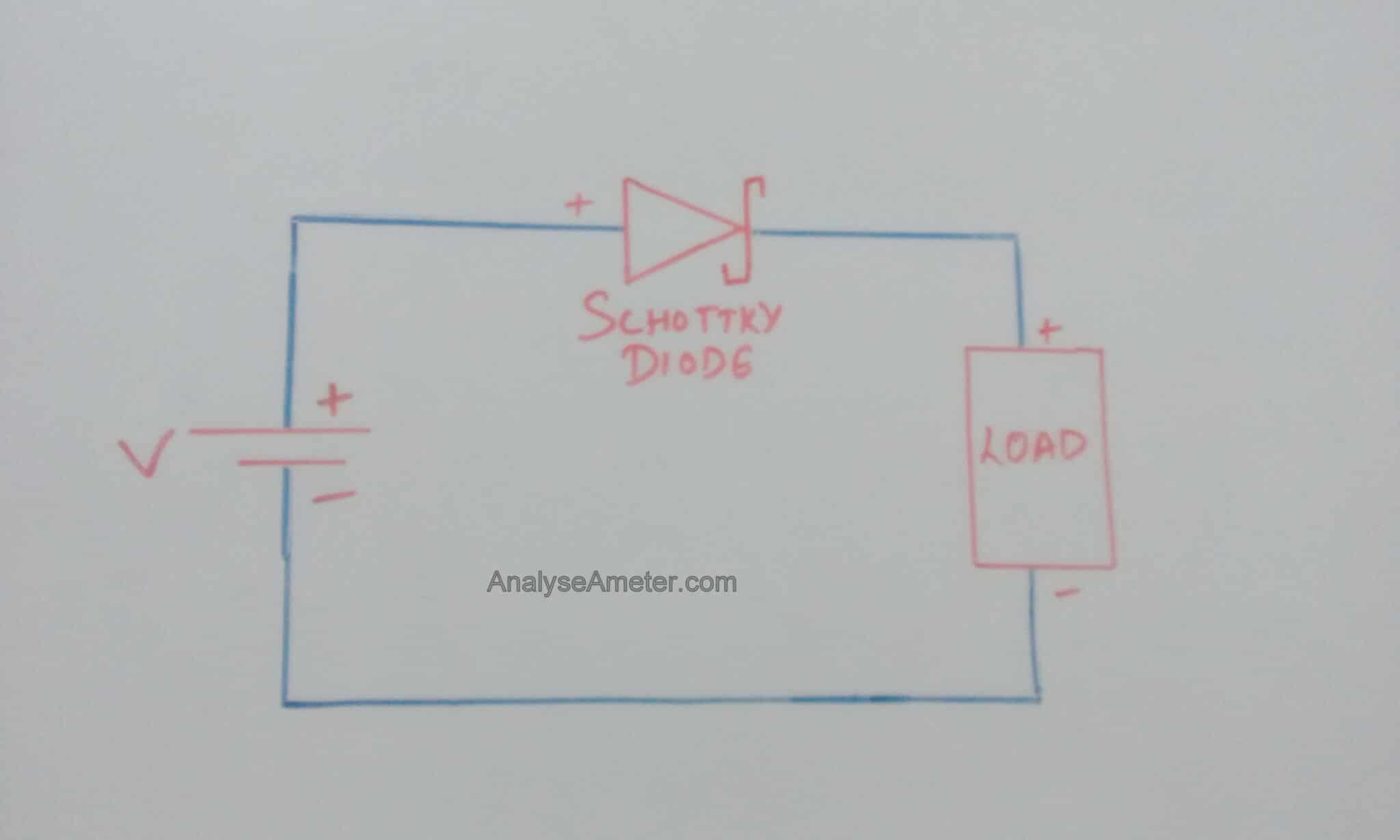
As shown in the figure above, voltage is applied to the Schottky diode in such a way that the metal is positive with respect to the semiconductor. It is a unipolar device because it has electrons as majority carriers on both sides of the junction. When these twos are brought in contact, electrons start to flow in both directions across the metal-semiconductor interface. Hence, there are no depletion region forms near the junction i.e. there is no significant current from the metal to the semiconductor with reverse bias. Due to electron-hole recombination time, the delay present in the junction diodes is absent. N-type semiconductors have higher potential energy as compare to electrons of metals. The voltage developed across the diode will oppose the built-in potential and makes easier to current flow.
Schottky Diode characteristics:
The VI characteristic of the Schottky diode is similar to a p-n junction diode with the following exception of forward voltage drop. The forward voltage drop of Schottky barrier diode is low as compare to the p-n junction diode.
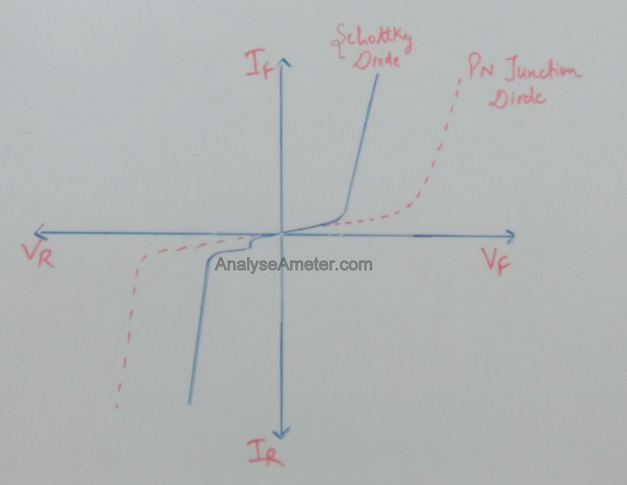
As shown in the figure above, the current rises exponentially with the increasing voltage in the forward direction having a knee or turn on the voltage of around 0.2V. In the reverse direction, there is a greater level of reverse current than that experienced using a normal p-n junction. Due to the high concentration of current carriers, the VI characteristics of this diode is steeper as compare to the normal diode. Into this diode, the forward voltage drop increases with the increasing doping concentration of n-type semiconductor.
Factors of Schottky diodes:
Before selecting Schottky diode for your work designers always consider working requirements of diodes because each and every diode works under specific operating conditions. Following important factors are:
(i) Operating Temperature margin: To keep a safe junction temperature margin from thermal runaway, the maximum operating junction temperature of the Schottky diode must be less than the maximum rating of the junction temperature in the data sheet.
(ii) Heat sink Temperature: Always use separate heat sinks for other components connected in series or parallel with Schottky diode because higher Tjmax class Schottkys allow a higher heat sink temperature. This temperature might be too high for other components on the same heat sink.
(iii) High ambient temperature: When we choose a Schottky diode with high rated Tjmax as ambient temperature increases, it will reduce the heat sink size.
(iv) Option of Tjmax class: A lower Tjmax class Schottky is the better choice but if the minimization of heat sink size is more important than minimization of energy losses then a higher Tjmax class Schottky is the better choice.
Schottky diode Applications:
Schottky diodes are the specially designed diodes used for many purposes. Following of its applications are:
- In high power application circuits, it is used as rectifiers.
- These diodes are often used as ant saturation clamps on transistors.
- In radio frequency applications it is used as mixer detector diode.
- In GaAs circuits, these diodes play a vital role.
- It is used in the stand-alone photovoltaic system to prevent batteries from discharging through the solar panels at night as well as in the grid connected system.
- It is used in voltage clamping applications.
- It is used in bipolar transistors TTL based 74LS ( low power schottky) and 74S (schottky) families of logic circuits.
Hope you all like this article. For any suggestions please comment below. We always appreciate your suggestions.
3 Comments