
PNP transistor and NPN Transistor are one of the most asked queries by students In this post, we are going to explain transistor working and its operation. Earlier we have covered its basics in the previous post of transistors where I have explained about what it is and its types. In short, “Transistors are the fundamental building block of modern electronic devices basically used for controlling, amplifying and generating electrical signals.” Before going on the working and operation part, let me first tell you about its construction.
Transistor construction:
A Transistor is a three layer semiconductor device in which one type of semiconductor (Either P-type or N-type) is sandwiched between two similar other types of semiconductor. The process of sandwiching is called fabrication of transistor.
Depending on the way of construction of transistor, it is of two types:
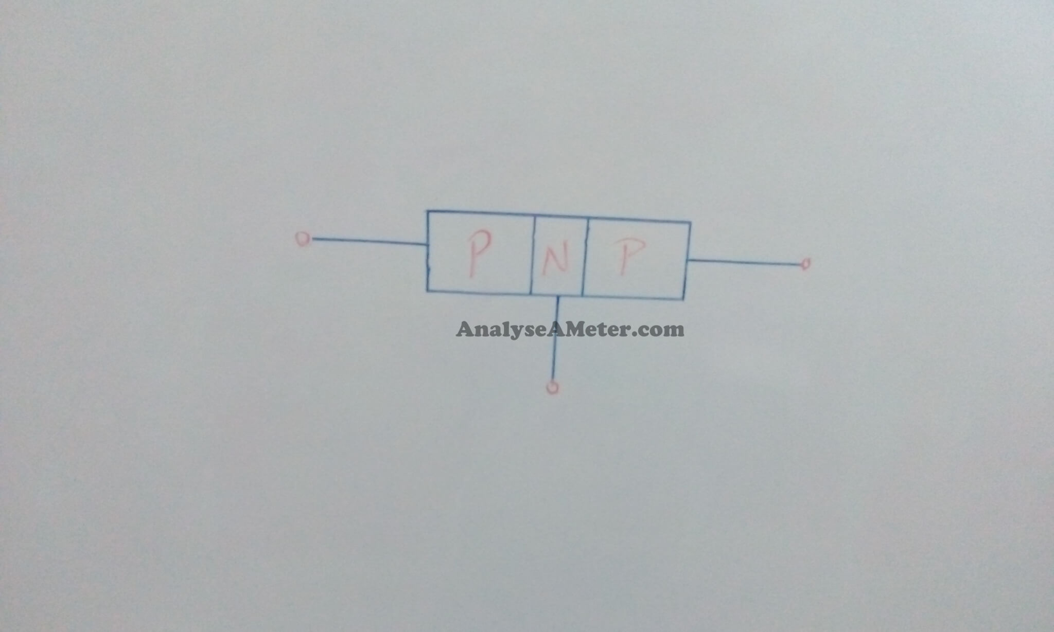
(i) PNP Transistor:
In this type of transistor, n-type semiconductor piece is sandwiched between two pieces of p-type semiconductor layers. The basic block diagram of PNP transistor is shown in the image below:
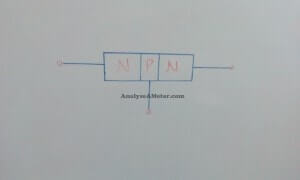
(ii) NPN Transistor:
As the Name suggests, in this type of transistor, p-type semiconductor piece is sandwiched between two pieces of n-type semiconductor layers. Look for the image below for its basic block diagram.
In each type of the transistor, the following points may be noted:
- Most important factor in the function of a transistor is the middle section which is present as a very thin layer.
- A transistor is a combination of two p-n junction, that’s why it is considered as a combination of two diodes connected back to back.
Useful Resources:
Transistor Terminals:
Transistors comprise of three sections of doped semiconductors. The portion on one side is the emitter and the portion on the opposite side is the collector. The Middle portion is known as the base which forms two junctions between the emitter and the collector as shown in the figure. These 3 are explained below in detail.
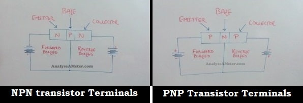
The 3 terminals of the transistor are explained briefly:
(i) Emitter: It is a heavily doped terminal through which electrons enter. It is always forward biased w.r.t. base so that it can supply a large number of majority carriers. As shown in the figure above, the emitter of PNP transistor (right side figure) is forward biased and supplies hole charges to its junction with the base while the emitter of NPN transistor (left side figure) supplies electron charges to its junction.
(ii) Base: It is lightly doped terminal through which electrons pass from the emitter to collector. The base-emitter junction is forward biased and allows low resistance to the emitter circuit while the base-collector junction is reverse biased and provides high resistance in the collector circuit. The Depletion layer is formed in the base junction of the transistor.
(iii) Collector: It is a moderately doped terminal which basically collects electron. The collector is always reverse biased and its function is to remove charges from its junction with the base. As shown in the figure above, the collector of the PNP transistor is reverse biased and receives hole charges that flow in the outer circuit while the collector of NPN transistor receives electron charges.
The whole thing will be clear once you read about the transistor working in this post. But before that, you must know about the symbolic representation of PNP and NPN transistors.
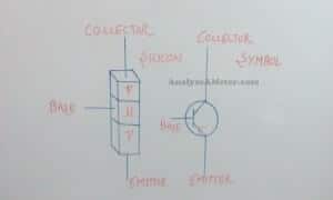
Transistor Symbols:
For the sake of convenience, the transistors are represented below by a schematic diagram.
The symbols of NPN and PNP transistors are shown distinctly. Basic transistor symbol is shown without the arrow (inward and outgoing). The arrow symbol shows the flow of current within the transistor hence representing if it is a PNP or NPN transistor.
-
PNP transistor Symbol:
In PNP transistor, the arrow is shown going inwards. The Emitter and collector junctions are positively charged due to the use of a P-type diode. While the base is negatively charged.
2. NPN transistor symbol:
Opposite of PNP transistor, in the NPN transistor, the arrow is shown going outward. The Emitter and collector junctions are negatively charged due to the use of an N-type diode. While the base is positively charged.
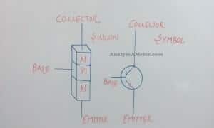
Note: The emitter is shown by an arrow which indicates the direction of flow of conventional current with the forward bias. In NPN transistor, the conventional current flows out of the emitter as indicated by the outgoing arrow while in PNP transistor the current flows into the emitter as indicated by the inward arrow.
Transistor Working and its operation
Basic Operation:
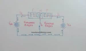
For an appropriate working of a transistor, the emitter-base junction is forward biased and the collector-base junction is reverse biased. For instance, if we ignore the emitter-base junction then practically due to reverse bias no current will flow in the collector circuit. However, if the emitter-base junction is also present then due to its forward bias emitter current starts to flow in the collector circuit. It is seen that this emitter current almost entirely flows in the collector circuit.
For e.g. if the emitter current is zero then the collector current is also zero while if the emitter current is 2mA then the collector current is also 2mA. This is the basic operation of a transistor.
Now we are going to explain the NPN and PNP transistor working. Have a look at it.
(i) Npn Transistor Working:

In this transistor, the forward bias causes the electrons in the n-type emitter to flow towards the base which constitutes the emitter current IE. When these electrons flow towards the base, it got combined with the majority carriers i.e. holes of the base. As we know, the base is very thin & lightly doped, therefore, to constitute base current IB only a few electrons i.e. less than 5% got combine with the holes. The remaining electrons i.e. more than 95% passes through the collector region to constitute collector current IC. In this way, the entire emitter current flows in the collector circuit. Therefore, it is clear that the emitter current is equal to the sum of collector current and base current i.e.
IE = IB + IC
(ii) PNP transistor working:
In this transistor, the forward bias causes the holes in the p-type emitter to flow towards the base which constitutes the emitter current IE. When these holes flow towards the base, it got combined with the majority carriers i.e. electrons of the base. As we know, the base is very thin & lightly doped, therefore to constitute base current IB only a few holes i.e. less than 5% got combine with the electrons. The remaining holes i.e. more than 95% passes through the collector region to constitute collector current IC. In this way, the entire emitter current flows in the collector circuit.
Note: Current conduction in NPN type transistor is by electrons while in PNP transistor is by holes.
Hope you all like this article. For any suggestions please comment below. We always appreciate your suggestions.
Thank you sir, great explanation.
Hi Muzaffar,
Thanks for commenting, If you have any problem related to electronics or electrical, you can ask in comments.
Thanks for the great explanation
Thanks Yashwanth for commenting.