

A transistor is one of the greatest inventions of the 20th century now used as a key element in all electronic circuits. In our previous article, we have talked in detail about the basics of a transistor. Here we are going to explain to you different transistor configurations in detail with their mathematical equations.
Types of Transistor configurations:
Transistors comprise three terminals i.e. Base, emitter, and collector. But when we connect it in a circuit, we require four terminals; two for the input and two for the output. To overcome this problem we make one terminal of the transistor common to both input and output terminals.
The input is fed between the common terminal and one of the other two terminals while the output is obtained between the common terminal and the remaining terminal. Based on this, a transistor can be configured in the circuit in the following three ways:
- Common Base Configuration
- Common Emitter Configuration
- Common Collector Configuration
Here we explain these configurations one by one in detail with its mathematical expressions. Have a look over it.
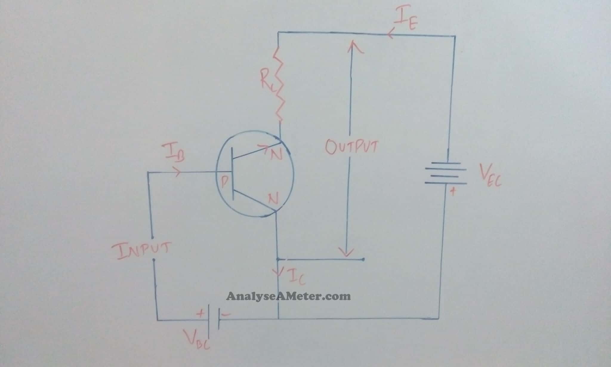
(i) Common Base configurations:
In this configuration, the base of the transistor is common to both input and output circuits. In its circuit arrangement, the input is applied between the emitter and base terminal, and output is taken from the collector and base terminal. The figure of common base NPN and PNP transistor is given below.
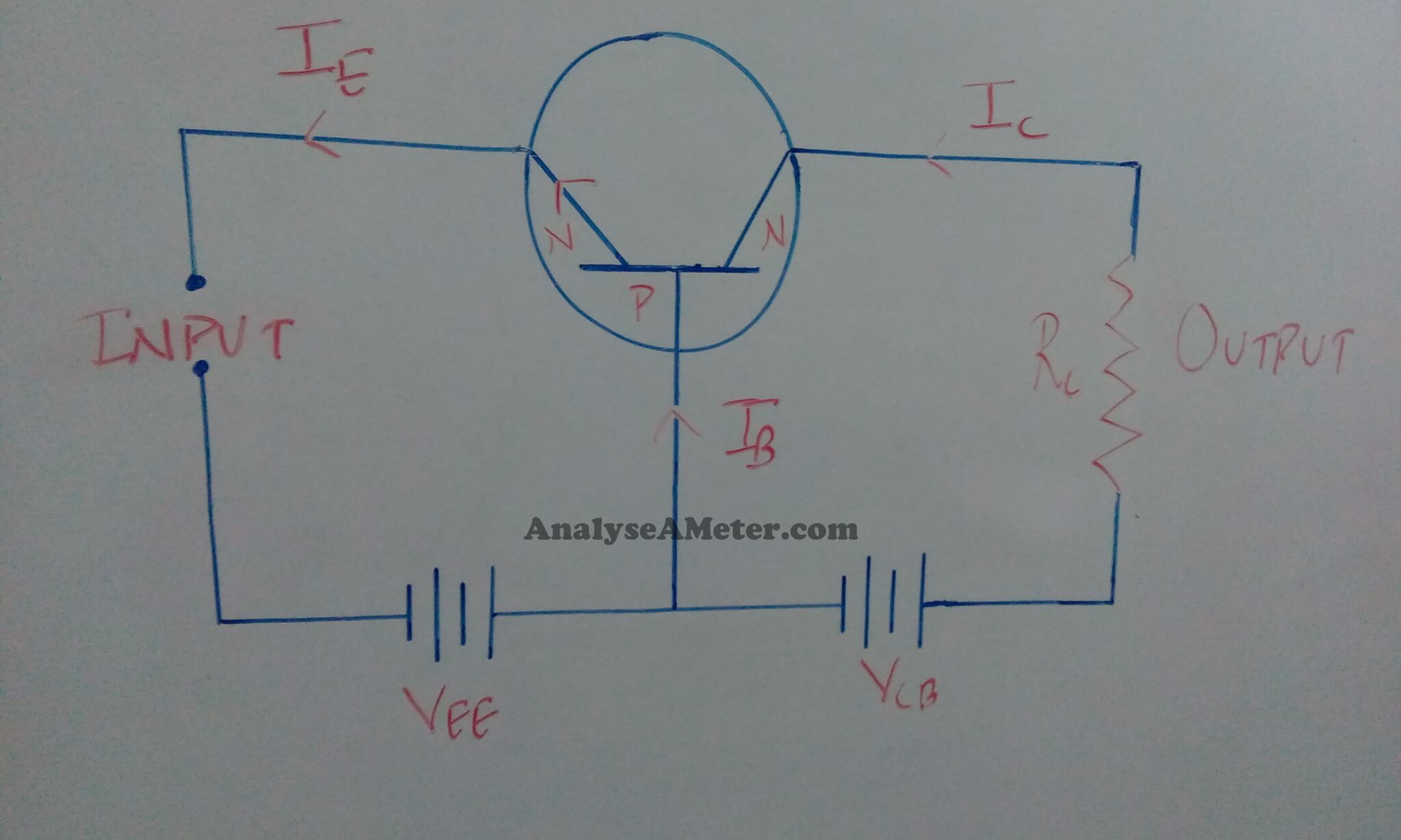 Common base configuration- NPN
(i) Current amplification Factor (α): The ratio of change in the collector current (Δ Ic ) to the change in emitter current (Δ IE ) at constant collector-base voltage VCB is known as a current amplification factor.
α = Δ Ic / Δ IE at constant VCB
From the above equation, it is clear that the current amplification factor is always less than unity. For commercial transistors, its value ranges from 0.9 to 0.99.
(ii) Calculation of collector current: As we know, the whole of the emitter current does not reach the collector because of the little bit electron-hole combinations takes place in the base area gives rise to base current. Furthermore, collector-base junction is reverse biased due to which some leakage current also flows because of minority carriers.
Therefore, the total collector current i.e. Ic is sum of the part of the emitter current which reaches the collector (α IE ) and the Leakage current (ILeakage )
Ic = α IE + ILeakage
If Ic = 0 then it is sure that some leakage current still flows in the collector circuit. This leakage current is abbreviated as Icbo means collector to base current with emitter open.
Therefore,
Ic = α IE + Icbo …. (i)
Ie = Ib + Ic
Ic = α ( Ib + Ic ) + Icbo
Ic = α Ib + α Ic + Icbo
Ic (1- α ) = α Ib + Icbo
Ic = α Ib / 1- α + Icbo / 1- α …. (ii)
By comparing equation (i) and (ii), you can calculate the value of Ic.
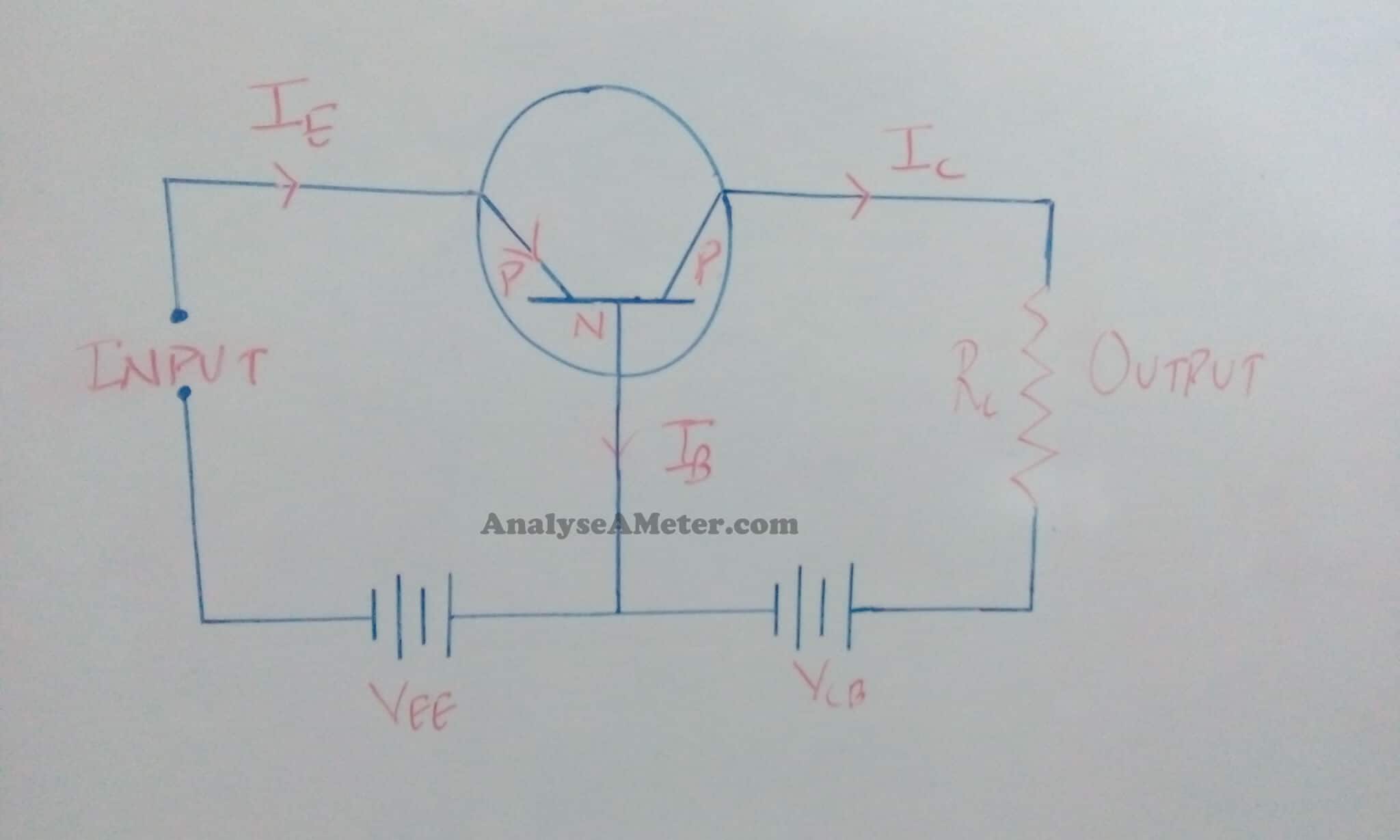
(ii) Common Emitter Configuration:
In this configuration the emitter of the transistor is common to both input and output circuits. In its circuit arrangement, the input is applied between the emitter and base terminal and output is taken from the collector and emitter terminal. The figure of common emitter NPN and PNP transistor is given below:
 Common emitter configuration- NPN
(i) Base current amplification factor ( β ) : In this configuration input current is Ib and output current is Ic. The ratio of change in collector current (Δ Ic ) to the change in base current (Δ Ib ) is known as base current amplification factor i.e.
β = Δ Ic / Δ Ib
In almost any transistors, less than 5 % of emitter current flows which indicates that the value of β is generally greater than 20 and its range lies between 20 to 500. We generally use this type of configuration because it gives tangible voltage gain and current gain.
Relation between β and α:
A Simple relation is established between β and α. This can be derived as follows:
β = Δ Ic / Δ Ib
α = Δ Ic / Δ IE
As we know,
Ie = Ib + Ic
Δ Ie = Δ Ib + Δ Ic
Δ Ib = Δ Ie – Δ Ic
Now put the value of Δ Ib in equation (iii), we get,
β = Δ Ic / Δ Ie – Δ Ic
Now divide the numerator and denominator by Δ Ie ;
β = (Δ Ic / Δ Ie ) / ( Δ Ie/ Δ Ie – Δ Ic/ Δ Ie)
As we Know,
α = Δ Ic / Δ IE
Therefore,
β = α / (1- α)
As per equation, it is clear that if α = 1 then β approaches infinity.
This indicates that the current gain in common emitter configuration is very high. Because of this reason this circuit arrangement is used in about 90-95 % of all transistor applications.
(ii) Calculation of collector current: The expression for collector current is derived as follows:
As we know,
Ie = Ib + Ic
Ic = α IE + Icbo
Ic = α ( Ib + Ic ) + Icbo
Ic = α Ib + α Ic + Icbo
Ic (1- α ) = α Ib + Icbo
Ic = α Ib / 1- α + Icbo / 1- α ….. (iv)
As shown in equation, if Ib = 0 i.e. the base circuit is open, then the collector current will be the current to the emitter. This is abbreviated as Iceo i.e. collector-emitter current with a base open.
Therefore,
Iceo = Icbo / 1- α
Substitute this value in equation (iv), then it becomes
Ic = α Ib / 1- α + Iceo
β = α / 1- α
Therefore,
Ic = β Ib + Iceo
With the help of this equation, you can easily calculate collector current by knowing the values of β Ib and Iceo.
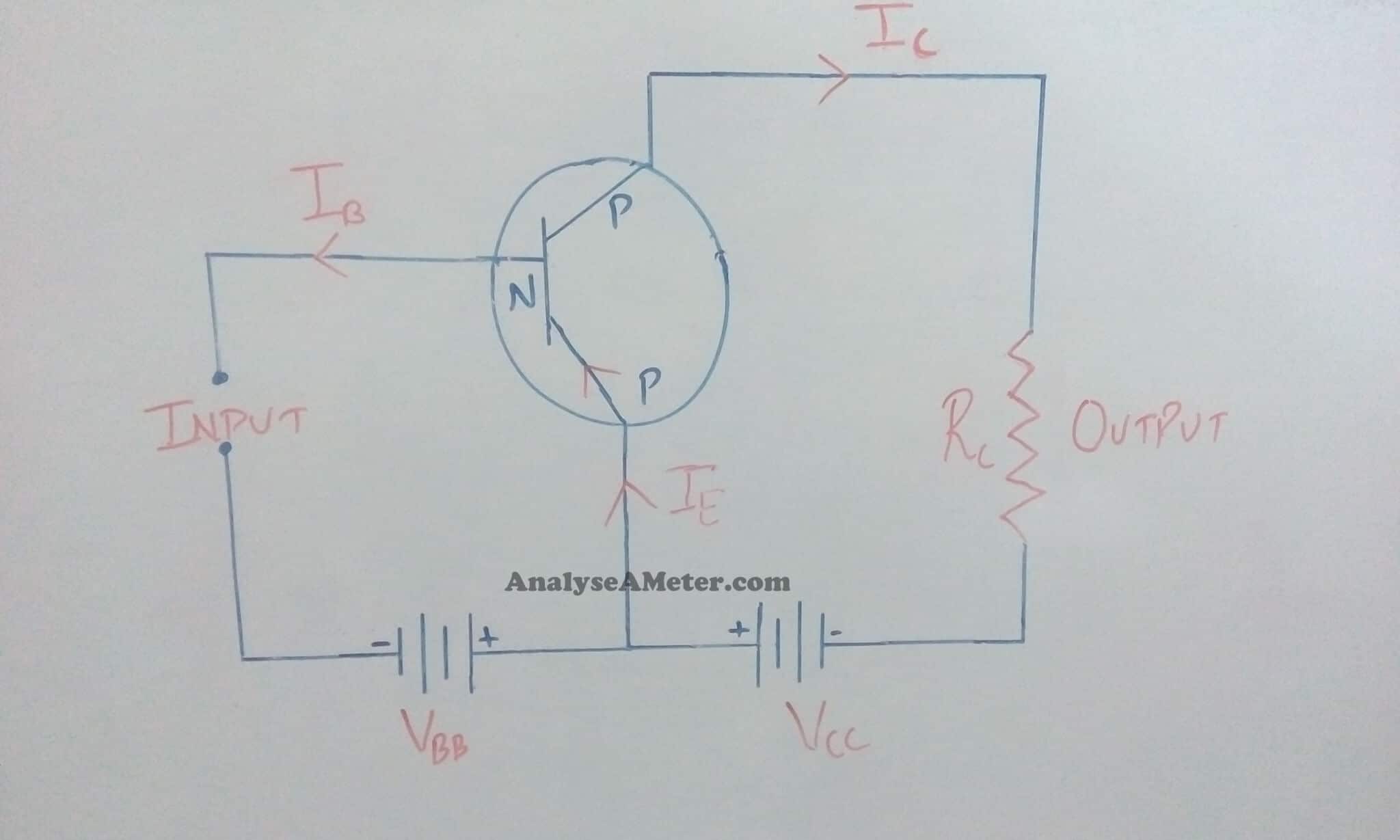
(iii) Common collector configuration:
In this configuration, the collector of the transistor is common to both input and output circuits. In its circuit arrangement, the input is applied between the base and collector terminal and output is taken from the collector and emitter terminal. The figure of common collector PNP and NPN transistor is given below:
 Common collector configuration- NPN

(i) Current amplification factor ( γ ) : In this configuration input current is Ib and output current is Ie. The ratio of change in emitter current (Δ IE ) to the change in base current (Δ Ib ) is known as base current amplification factor i.e.
γ = Δ Ie / Δ Ib
The Current gain of this circuit is same as the common emitter circuit i.e. Δ Ie ≈ Δ Ic. Hence, its voltage gain is always less than 1.
Relation between γ and α :
As we know,
γ = Δ Ie / Δ Ib …. (v)
α = Δ Ic / Δ IE
Ie = Ib + Ic
Δ Ie = Δ Ib + Δ Ic
Δ Ib = Δ Ie – Δ Ic
Put the value of Δ Ib in equation (v);
γ = Δ Ie /( Δ Ie – Δ Ic )
Now divide the numerator and denominator by Δ Ie ;
β = (Δ Ie / Δ Ie ) / ( Δ Ie/ Δ Ie – Δ Ic/ Δ Ie )
As we Know,
α = Δ Ic / Δ IE
Therefore,
γ = 1 / 1- α
By knowing the value of α, you can easily calculate the value of γ.
(ii) Calculation of Collector current: The expression for collector current is derived as follows:
As we know,
Ic = α IE + Icbo
Ie = Ib + Ic
Put the value of Ic in the above equation;
Ie = Ib + α Ie + Icbo
Ie (1- α ) = Ib + Icbo
Ie = Ib / (1- α ) + Icbo / (1- α )
β = α / 1- α
If we add 1 on both L.H.S and R.H.S then this equation becomes;
(β + 1) = α / (1- α ) + 1
By calculating,
(β + 1) = 1 / (1- α) = γ
Therefore,
Ie = (β + 1 ) Ib + (β + 1 ) Icbo
As we know,
Δ Ie ≈ Δ Ic
Therefore,
Ic = (β + 1 ) Ib + (β + 1 ) Icbo
From this expression, you can easily calculate the collector current.
Note: Voltage gain provided by this circuit is always less than 1 because it has very high input resistance and very low output resistance. Due to high input resistance and low output resistance, this circuit is used for Impedance matching and amplification purposes.
Hope you all like this article. For any suggestions please comment below. We always appreciate your suggestions.
Can you please tell me difference between common emitter and common base configuration based on current gain,voltage gain,applications,and output wave form.
Please reply