
Transistors are a widely used component in an electrical circuit. We have already discussed FET (Field effect transistors) and JFET (Junction Gate Field-effect transistors) in our previous tutorials. Another most used Transistor is Mosfet. In this tutorial, we will explain its definition, working modes, operation, and types.
What is Mosfet: Definition and explanation
According to Wikipedia
The metal–oxide–semiconductor field-effect transistor (MOSFET, MOS-FET, or MOS FET) is a type of field-effect transistor (FET), most commonly fabricated by the controlled oxidation of silicon. It has an insulated gate, whose voltage determines the conductivity of the device
Let’s understand this definition of Mosfet in simple terms:
- Mosfet Transistor or Metal Oxide Semiconductor Field Effect Transistor is a voltage controlled field effect transistor.
- It has a metal oxide gate electrode.
- The gate electrode is electrically insulated from the main semiconductor n-channel or p-channel by a very thin layer of insulating material.
- The insulating material is a silicon dioxide also known as glass.
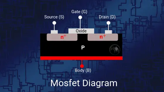
- It has 4 terminals namely: Body (B), Drain (D), Gate (G), and Source (S).
Note:
The Body of Mosfet is connected to its source hence making it a 3-terminal FET.
So we can sum up the above points as “Metal Oxide Semiconductor Field effect transistor is a semiconductor device which is voltage controlled. It has 3 terminals and 2 working modes namely P-channel and N-channel. It uses a metal oxide gate electrode which is electrically insulated from the main semiconductor by insulating material; Silicon dioxide (SiO2) also known as glass“.
Mosfet Basics
MOSFETs generally work by electronically varying the width of a channel through which charge carriers i.e. electrons or holes travels because the device conduction is directly proportional to the channel width. The wider the channel, the better the device conducts.
Mosfet terminals
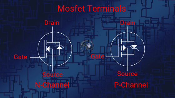
Like Jfet, Mosfet is a three terminal device i.e. source, drain and gate. The charge carriers either holes or electrons enters through the source terminal and exits through the drain terminal. The channel width is controlled by the voltage applied to the electrode i.e gate present between the source and Drain terminal which is insulated from the channel by a thin layer of metal oxide.
Note: Just like Jfet, Mosfet is also considered as a voltage controlled resistor because the current flowing the main channel between the source and drain is proportional to the input voltage.
Mosfet Symbols
Generally, a variety of symbols is available for Mosfet’s. It operates in two modes; enhancement mode and depletion mode. As shown in Figure three line segments are used for enhancement mode and a solid line is for depletion mode.
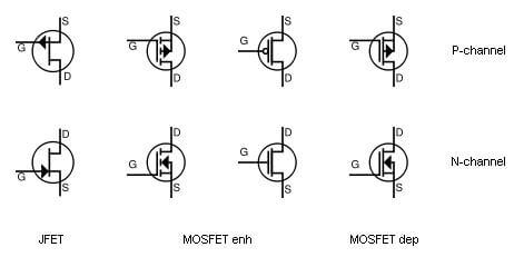
Mosfet symbol used above indicates that the device has a bulk substrate- indicated by the arrow on the central area of the substrate. The Substrate is the fourth terminal which is not normally used as either an input or output connection but instead used for grounding the substrate while in discrete type Mosfet substrate lead is connected internally to the source terminal.To the body or metal tab of the Mosfet, the substrate connects to the main semiconductive channel through a diode junction.
The Semiconductive channel is the channel between the source and drain through which majority carriers travel. As shown in the figure, if this is a solid unbroken line then it represents a Depletion (normally ON) type Mosfet while If the channel line is shown dotted then it represents an Enhancement (normally OFF) type Mosfet. The direction of the arrow indicates whether the conductive channel is a p-type or an n-type semiconductor device.
Mosfet operation:
Metal oxide semiconductor field effect transistor structure is obtained by growing a layer of silicon dioxide (Sio2) on top of a silicon substrate and depositing a layer of metal or polycrystalline silicon. When a voltage is applied across the MOS structure, the majority or minority carriers start moving inside the semiconductor depends upon the polarity i.e. p-type or n-type.
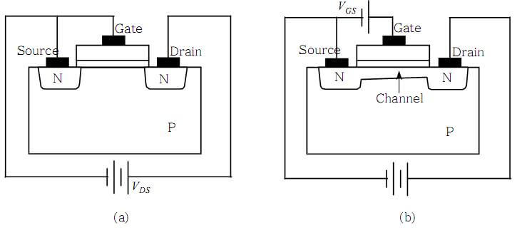
Let us take the example of p-type semiconductor. When we apply the positive voltage across the gate to body (Vgb) terminal then the positive charge holes start moving away from the gate/insulator semiconductor interface, leaving behind the negatively charged acceptor ions which results in the formation of the depletion layer. If we further increase the voltage across the gate to body (Vgb) terminal then the high concentration of negative charge carriers starts forming in an inversion layer. Conventionally, the gate voltage at which the volume density of electrons in the inversion layer is same as the volume density of holes in the body is called the Threshold voltage. When the voltage between the transistor gate and source exceeds the threshold voltage then it is known as overdrive voltage.
Mosfet types:
Today’s Mosfet is used in many applications such as in electronic switches or to make logic gates because with no bias they are normally non-conducting. Both the p-channel and n-channel MOSFETs are available in two basic forms; one is Depletion mode and another is Enhancement mode.
(i) Depletion mode Mosfet:
Being a depletion mode device, normally on Mosfet type acts as normally closed switch and requires no gate current to function. In depletion mode MOSFET, we apply more negative voltage than the threshold voltage which depletes or shutting off the majority current carriers in the preformed channel beneath the gate. As a result, the size of the depletion region got changed which further increase the channel resistance and reduce the current flow.
In p-channel depletion MOS transistor a positive gate-source voltage +Vgs will turn off the transistor by depleting the channel of its free holes while in n-channel depletion MOS transistor a negative gate-source voltage -Vgs will turn off the transistor by depleting the channel of its free electrons.
In n-channel depletion mode:
- +Vgs means more electrons and more current.
- -Vgs or zero voltage less electrons and less current.
In p-channel depletion mode:
- +Vgs means fewer electrons and less current.
- -Vgs or zero voltage more electrons and more current.
(ii) Enhancement mode Mosfet:
Enhancement mode Mosfet is the reverse of the depletion mode type into which the conducting channel is lightly doped which remains the device normally off when the gate bias voltage Vgs is equal to zero.
In n-channel enhancement Mos transistor, when a gate voltage is applied to the gate terminal greater than the threshold voltage level then the drain current will start flow which making it a transconductance device.
In n-channel enhancement mode:
- +Vgs turns the transistor ON
- -Vgs or zero voltage turns the transistor OFF
In p-channel enhancement mode:
- +Vgs turns the transistor OFF
- -Vgs or zero voltage turns the transistor ON
Hope you all like this article. For any suggestions please comment below. We always appreciate your suggestions.
One Comment