Pn junction diodes are a kind of basic diodes formed by using two types of extrinsic semiconductors i.e p-type and n-type semiconductors. So that these can show properties of both depending upon the biasing of the circuit.
We have discussed semiconductors in detail with the Energy band diagram if you want to read about it’s working, types and biasing you can go to our detailed semiconductor guide.
In this article though, we will discuss p-n junction formation, Diffusion, Depletion region, and drift phenomenon and basic equation.
What is PN Junction
Pn junction is an interface, typically a joint between two adjoining semicondictors. It is formed by joining two different types of semiconductor material i.e. p-type semiconductor on one side and n-type semiconductor on another side. The process of formation of Pn junction is called “fabrication of Pn Junction”.
[su_note note_color=”#FF0000″ text_color=”#ffffff”]Extra Marks: PN Junction was discovered by the American physicist Russell Ohl at Bell laboratories.[/su_note]
What is the use of PN Junction?
As we have read in our article on semiconductor (link given above), in p-type semiconductor holes are majority carriers and electrons are minority carriers and these works only when it is connected to the positive terminal of the circuit. Similarly, an n-type semiconductor works when connected to the negative terminal of the circuit because it has electrons as majority carriers and holes as minority carriers. So we can say they work in a particular condition only.
But when these semiconductors are joined chemically i.e. fabricated the product shows different behavior. The electrons and holes get attracted and repelled towards the center according to the power source connection. This results in the formation of the depletion layer and different regions (explained below).
Due to which some properties like resistance, breakdown temperature, breakdown voltage and characteristics, etc get changed and diode exhibits differently according to the biasing of PN Junction Diode. And we can use a single junction for negative and positive both types of voltage supply.
P-n junction formation/ Fabrication of PN Junction
As we know the elements around us are classified into three categories i.e. insulator, conductor, semiconductor, etc depending upon their electrical conductivity. According to the Energy Band theory (explained in Semiconductor guide), the conductivity of semiconductors lies between conductors and insulators i.e. conductors have high electrical conductivity and insulators have low electrical conductivity.
The most common semiconductors we are using for the formation of PN junction are Germanium and silicon because of its electrical properties.
Generally, there are several different ways to make a p-n junction. For the ease of understanding, we are explaining it in a simpler way by taking an example.
We usually make PN junction using a single wafer of Pure Silicon or Germanium. For the formation of the p-n junction, we first convert a silicon wafer to a p-type semiconductor by doping it with a trivalent impurity i.e. aluminum, gallium, etc on one side.
Then we dope this same p-type semiconductor with a pentavalent impurity i.e. antimony, phosphorus, etc to form an n-type region on the same wafer. Hence making p-type and n-type semiconductors on the same wafer.
This technique is called Fabrication of PN junction which results in the formation of the junction.
Diffusion, Depletion, and Drift in PN Junction
At the time of PN junction formation, we observe different phenomena that occur like the movement of the majority and minority carriers, region formation, etc. Knowledge of these phenomenons is very important to understand other topics like VI characteristics of PN Junction (discussed in PN junction diode article, link given above) and different types of diodes and their applications.
Three important phenomena that occur during the formation of the p-n junction are:
(i) Diffusion:
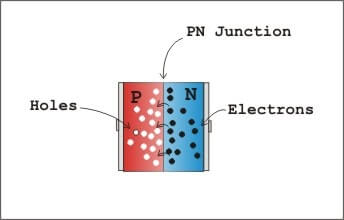
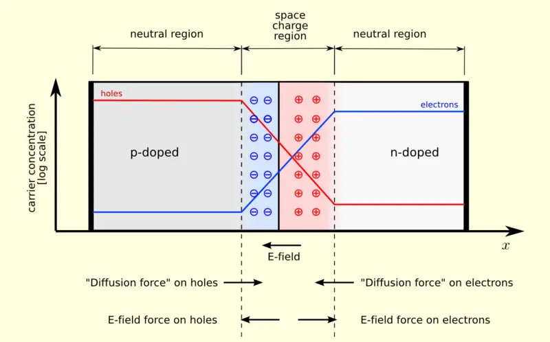
In a silicon wafer when the junction is formed, a movement in charge carriers occurs between p-type and n-type materials due to the unequal distribution of holes and electrons in the semiconductor. This depends solely on the concentration of charge carriers. This results in the movement of electrons from the n-side to the p-side and holes from the p-side to the n-side through the junction.
Similarly, when a hole is diffused to the n-side it leaves behind an ionized acceptor at the p-side and when the electron leaves the n-side region, it leaves behind an ionized donor at the n-side.
This movement of electrons from the n-side to the p-side and the holes from the p-side to the n-side is called Diffusion which results in diffusion current.
(ii) Depletion Layer/ Region formation:
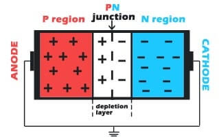
As we know, when more and more electrons leave the n-region and more and more holes leave the p-region then a region of positive and negative charges is formed at the junction. Negative charges get deposited near the p-side junction and the positive charges get deposited near the n-side junction.
The region where negative and positive charges get deposited on one of the sides is known as a depletion region. (Read Q-A below to know the full process with diagram)
(iii) Drift Current:
When the negative charges get deposited near the p-side junction and the positive charges get deposited near the n-side junction then the electric field is generated. This electric field causes electrons to move from p-side to n-side and the holes from n-side to the p-side. This motion of charge carriers due to the electric field is known as drift and the current resulting from the flow of electrons and holes is known as drift current.
[su_note note_color=”#ff0000″ text_color=”#ffffff”]Extra Marks: Drift current is opposite in direction to the diffusion current.[/su_note]
Width of Depletion Region in PN Junction (Equation)
In p-n junction, the size of the depletion region depends on the movement of the majority and minority carriers. Here we are explaining it with the help of a mathematical equation also known as the depletion region equation.
Depletion Region Width (d)
Let us assume, Ca and Cd are the concentration of acceptor and donor atoms
And No and Po is the equilibrium concentration of electrons and holes respectively.
As per the poison’s equation:
-d2 V / dx2 = ƿ / ϵ
= q / ϵ [ (No – Po) + (Ca – Cd )
Where,
V= Electric potential
Ƿ = Charge Density
ϵ = Permittivity
q = Magnitude of electron charge
As we know, the total charge on either side of the depletion region must cancel out. Therefore, the multiplication of the width and the concentration on the p side and the n side becomes equal i.e
dp Ca = dn Cd
Where,
dp = width of depletion region within the p-side
dn = width of depletion region within the n-side
After the movement of majority and minority carriers, the entire depletion region and potential difference (∆ V) across the p-n junction can be calculated as given below;
∆ V = ʃD ʃ q / ϵ [ (No – Po) + (Cd – Ca ) dx dx
= (Ca Cd / (Cd – Ca ) )x (2q (dp + dn )2 / ϵ )
But in the depletion region, the value of No and Po is equal to zero.
Therefore, the total width of the depletion region can be defined as:
d = √ (2 ϵ (Ca + Cd )/ q Ca Cd ) x ∆V
where ∆V can be written as ∆Vo + ∆Vext i.e. it is split into the voltage difference into the equilibrium plus external components.
Check animation of PN junction to gather more information: PN junction video
PN Junction FAQs
Q1: How is PN Junction formed?
Ans: There are many techniques to form a PN junction. But in the easiest way, it is formed by the doping of a single Pure Semiconductor with p-type and n-type impurities. The process is called the fabrication of PN Junction.
Q2: Explain the diffusion phenomenon in PN Junction?
Ans: Diffusion is a process of equalization of charge carriers. It occurs due to the unequal concentration of charge carriers in the wafer. Once the charge carriers get equal at both sides of the wafer, the process of diffusion stops. It doesn’t depend on external forces. The current produced by this process is called diffusion current.
Q3: What is Drift in PN Junction?
Ans: Unlike Diffusion, the Drift phenomenon depends on external force. The process of drift in charge carriers starts when we apply an external voltage source to the wafer or diode. Here, drift means the charge carriers start moving due to external voltage supply depending on the biasing. This produces drift current in the junction or diode.
Q4: What is a difference between Diffusion current and Drift current in PN Junction?
Ans: There is a vast difference between diffusion and drift current. We will take them pointwise:
- Drift current occurs due to the movement of charge carriers by an external source, Diffusion current occurs naturally.
- Drift current depends on the electric field while Diffusion current depends on diffusion coefficients, a proportionality factor, and charge of holes and electrons.
- The direction of drift current depends on the biasing while the direction of Diffusion current is in the opposite direction to the movement of electrons and in the same direction as of holes. That means, the direction of diffusion current depends on the direction of the change in the carrier concentration.
Q 5: Does diffusion and Drift current contributes to the total current of a diode?
Ans: Yes, both Diffusion and drift current contribute significantly in the calculation of total current in the diode.


2 Comments