
FET or field-effect transistor is a three-terminal unipolar semiconductor device. It is used for amplification of weak signals. This type of transistor basically uses an electric field to control the shape and hence the electrical conductivity of a channel of one type of charge carrier in a semiconductor material.
FET has various similar characteristics to those of their bipolar transistor counterparts i.e. robust, cheap, high efficiency and instant operation and can be used in various electronic circuit applications. In our previous article, we explain the difference between BJT and FET, Semiconductors electronics Theory. Here we are going to explain FET operation and its types.
What is Fet Transistor or Field Effect Transistor
Field-effect circuits are used in many areas of electronics involves single carrier type operation i.e. unipolar in nature. Fets can be minority carrier charge devices if the current is carried out by minority carriers or majority carrier charge devices if the current is carried out by majority carriers.
In Fet, the current flows through the semiconductor path is known as a channel. There are different types of electrodes on both sides of the channel. The physical diameter of the channel is fixed but its effective electrical diameter can be varied by the application of a voltage to a control electrode Known as a gate. At given instant of time, the conductivity of field effect transistor depends on the electrical diameter of the channel.
(A) FET terminals:
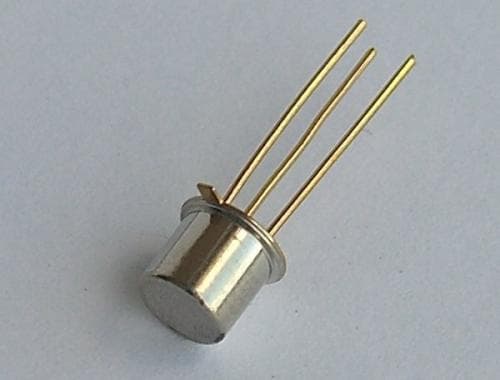
FET transistors come in large variety of packages and all of them are susceptible to ESD or electrostatic discharge. It has three terminals:
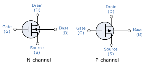
(i) Source: Through this terminal the majority carriers enter the channel i.e. it act as the source of carriers for the device. The current entering the channel through the source S is denoted by Is.
(ii) Gate: This terminal controls the channel conductivity and is denoted by G. By applying the voltage to G, one can control Ig.
(iii) Drain: Through this terminal the majority carriers leave the channel i.e. they are drained from the channel. The current entering the channel through the drain D is denoted by Id. Its drain to source voltage is denoted by Vds.
(B) FET Channels:
By applying the voltage across the gate and drain terminals, the electrons or holes starts moving from the source to drain terminal and affects the size and shape of a conductive channel. The flow of electrons or holes through the source to drain is generally control by the FET.
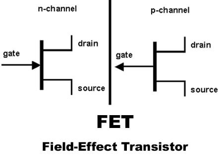
Field effect transistor is N channel or P channel device operates in two modes i.e. depletion mode and enhancement mode. Here we discuss N channel and P channel FET device in detail.
(i) N-channel:
In n-channel depletion mode device, we always apply a negative gate to source voltage which causes a depletion region to expand in width and narrowing the channel. If the width of the region further expands, then the resistance of the channel become large from source to drain cause the FET turned off like a switch. This is known as pinch-off and the voltage at which it occurs is called the pinch off voltage.
In n-channel enhancement mode device, we apply positive gate to source voltage because in this mode no conductive channel exists within the transistor. Applied positive voltage attracts the electrons within the body towards the gate forms a conductive channel. The applied voltage is known as the threshold voltage which attracts the enough electrons near the gate to counter the dopant ions and form a region known as depletion region.
(ii) P-channel:
In p-channel depletion mode device, we apply a positive voltage from gate to source which creates depletion layer by forcing positively charged holes away from the gate insulator interface.
(C) FET operation:
In FET enhancement mode or depletion mode devices, drain to source voltages is always less than the gate to source voltages and drain current will be proportional to drain voltage.
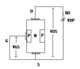
As shown in Figure above, the gate is always in reverse biased, hence, the gate current Ig is practically zero. When a voltage is applied to the gate, the charge carriers start moving from source to drain. The source terminal is connected to end of the drain supply which provides the necessary charge carriers in N-channel JFET source terminal. When the electron starts moving through the channel from drain to source, the current Id increases as Vds increased from zero. This relationship between Vds and Id continuous till Vds reaches certain value called pinch-off Vpo. If we increase drain to source voltage further, the pinch off point of the channel begins to move away from the drain towards the source, hence FET is said to be in saturation mode.
Types of Field effect Transistor:
Field effect transistor is of two types:
(i) JFET: Junction gate field effect transistor is a three terminal semiconductor device can be used as electronically controlled switches, voltage controlled resistors and amplifiers. JFets can have an n-type or p-type channel. It is usually on when there is no potential difference between its gate and source terminals.
(ii) MOSFET: Metal oxide semiconductor field effect transistor is a four terminal device used for amplifying or switching electronic signals. As compare to regular transistors, MOSFET requires very little current to turn on and delivering much higher current to a load.
Hope you all like this article. For any suggestion comment below.We always appreciate your suggestions.
5 Comments