BJT and FET both are made up of different semiconductor materials mainly P type and N type. These transistors are basically used for the designing of oscillators, amplifiers, and switches. In our last articles, we explain in detail how to use a transistor as a switch, amplifier and as an oscillator.
Here we are going to explain in detail about FET and BJT basics, working and its difference.
Bipolar Junction transistor:
Bipolar transistor is a three terminal device formed by joining two individual signal diodes back to back, which will give us two PN junctions connected together in series that share a common p-terminal or n-terminal.
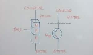
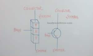
By the application of a small signal voltage these transistors act as either an insulator or conductor. It has three-terminals namely; emitter, base, collector. In our previous articles, we explain in detail transistor construction and working.
These transistors have an ability to operate within three different regions:
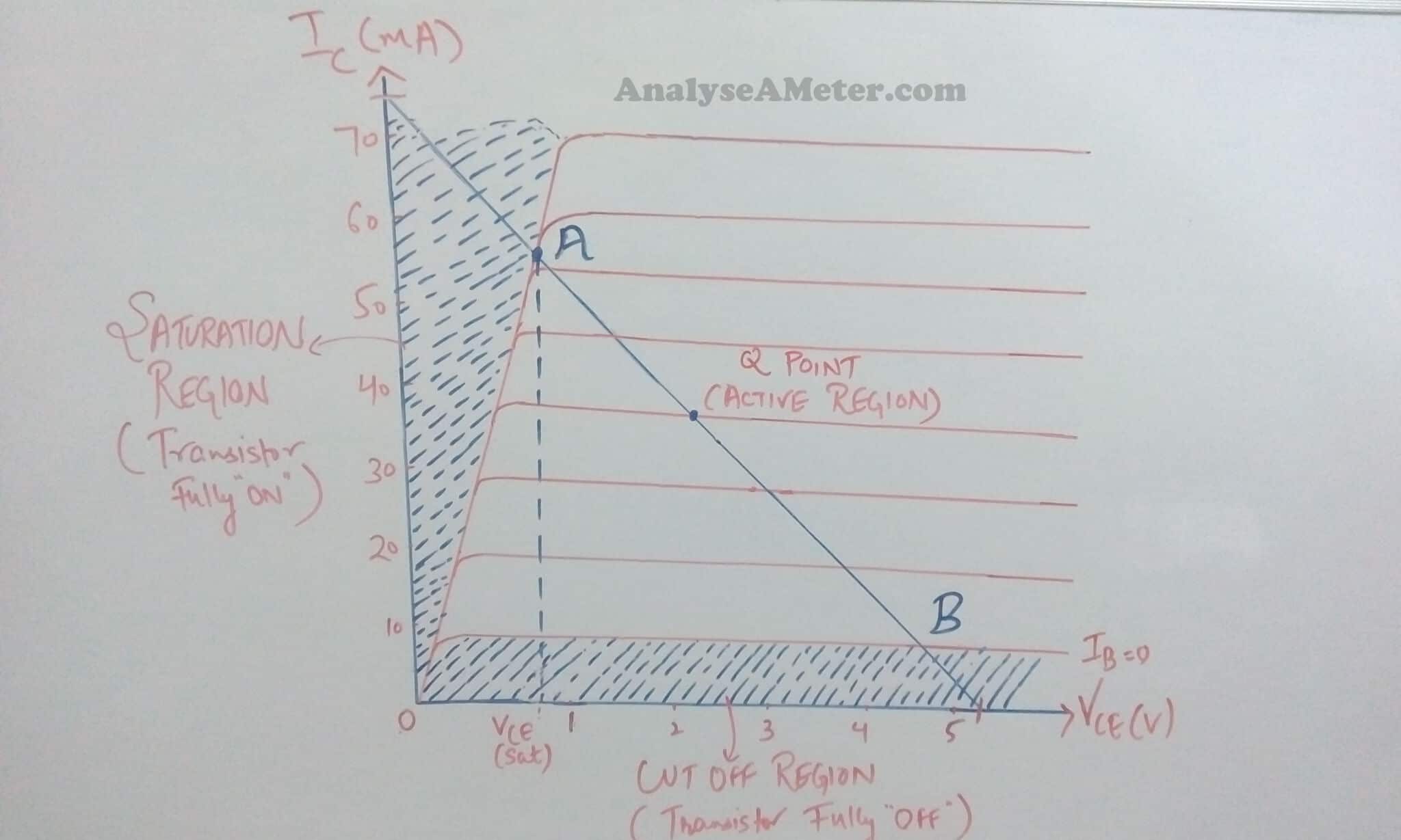
(i) Active Region: Transistor is basically operated in active region when the emitter-base junction is forward biased and the collector-base junction is reverse biased. In this region transistor operates correctly and act as an amplifier i.e. Ic = β Ib.
(ii) Saturation Region: Transistor is said to be operated in the saturation region when both the emitter-base and collector-base junction are forward biased. In this region, the collector current increases rapidly for a very small change in collector voltage. In this region transistor is “ Fully On” operating as a switch and Ic = I (Saturation).
(iii) Cut off Region: Transistor is said to be operated in the cut-off region when both the emitter-base and collector-base junction are reverse biased. In this region, the current in the transistor is very small and thus the transistor is assumed to be in off state. In this region transistor is “Fully Off” operating as a switch and Ic = 0.
(iv) Reverse active region: Transistor is basically operated in this region when the emitter-base junction is reverse biased and the collector-base junction is forward biased. In this region transistor will not operate correctly and obtains a very poor output.
It is of two types i.e. NPN and PNP. In NPN transistor, electrons are majority carriers and holes are minority carriers while in PNP transistor holes are majority carriers and electrons are minority carriers.
Note: We are using NPN transistors most because electrons are more mobile than holes and constitute more current as compared to holes.
Field effect transistors:
Field effect transistor is a transistor that uses an electric field to control the shape and hence the electrical conductivity of a channel of one type of charge carrier in a semiconductor material. These transistors are commonly used for weak signal amplification i.e. amplify digital signals and analog signals.
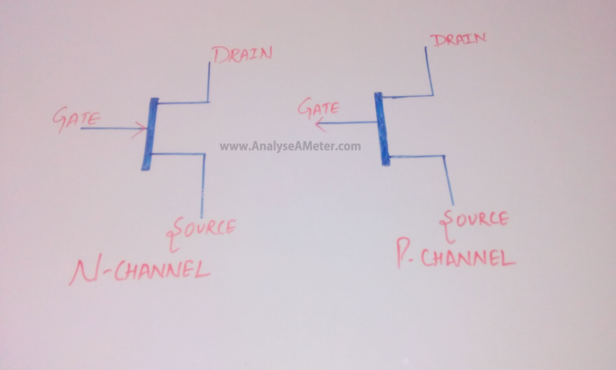
The Fet’s three terminals are:
- Source: Through this terminal the carriers enter the channel and conventionally the current entering the channel at S is designated by Is.
- Drain: Through this terminal the carriers leave the channel and conventionally the current entering the channel at D is designated by Id.
- Gate: This terminal modulates the channel conductivity. By applying a voltage to G, one can control Id.
The conductivity of the FET depends on the diameter of the channel. A small change in gate voltage can cause a large variation in the current from the source to the drain. This is how the Fet amplify a signals.
Types of Field effect transistor
Field effect transistors are also known as unipolar transistors because they involve the single carrier type operation. The conductivity of FET is regulated by a voltage applied to a terminal which is insulated from the device. These are of two types:
- JFet ( Junction Field effect transistor): It is a voltage controlled device in which current flows from the source terminal ( equivalent to the emitter in a bipolar transistor) to the drain (equivalent to the collector). The voltage applied between the source terminal and the gate terminal is used to control the source-drain current.
- MosFet (Metal oxide semiconductor Field effect transistor): It is a voltage controlled field effect transistor has a metal oxide gate electrode which is electrically insulated from the main semiconductor n-channel or p-channel by a very thin layer of insulating material commonly known as silicon dioxide or glass.
Difference between the BJT and FET:
In electronic circuits, Field effect transistors can be used to replace normal Bipolar junction transistors. In the table below we explain the basic differences between the BJT and FET.
| Bipolar Junction Transistor | Field Effect Transistor |
| BJT has 3 terminal; emitter, base and collector | FET’s 3 terminals are Source, drain and gate |
| BJT is a Bipolar transistor | FET is a Unipolar transistor |
| Cost is cheaper | Expensive in cost |
| Large in size | Small in size |
| Output impedance is Low | Output impedance is high |
| Input impedance is Low | FET has Very HIGH impedance |
| Generates Medium Noise | Generates low noise |
| Biasing process of BJT is easy | Biasing process of FET is easy |
| It has High Voltage Gain | It has Low Voltage Gain |
| It has Low Current Gain | It has High Current Gain |
| Switching time is Medium | Switching time is Fast |
| BJT is Robust in nature | FET can be damaged easily |
| Less Temperature stability | High Temperature stability |
| It is a current-driven/controlled device | It is a voltage-driven/controlled device |
Hope you all like this article. For any suggestions please comment below. We always appreciate your suggestions.


2 Comments