

Electronic Transistors are small devices that are used to control the flow of current in the circuit.
Transistor is a very important electronic component used in circuits because it can be modified to act as other various electronic components such as a switch, Oscillator, etc.
In a same way we can use a transistor as an amplifier. It is used when the input signal in a circuit is weak.
We have written an extensive and easily understandable guide on Electronic Transistor and working of transistor. We recommend you to go through these articles before reading ahead.
So, here in this article, we are going to explain Transistor as an amplifier.
Transistor as an Amplifier
Transistor amplifier is an arrangement where we configure NPN transistor in common emitter configuration of a transistor.
A Transistor circuit that can raise the strength of the input signal in the circuit is known as Transistor amplifier. It is also known known as Common Emitter Transistor or Amplifier.
The explanation of working of transistor amplifier involves the knowledge of amplification and amplifier. I strongly recommend reading our articles on Amplifier circuit theory.
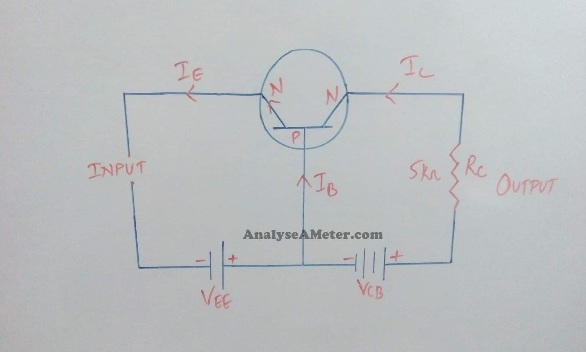
The above diagram shows the basic arrangement of NPN Transistor as a transistor amplifier.
As shown in the figure above, we apply input signal which has weak strength between the emitter-base junction and takes the output across the load Rc connected in the collector circuit.
For maximum amplification, always ensure that the input circuit is forward-biased and the output circuit is reverse-biased.
For this purpose, we apply D.C voltage i.e. VEE in the input circuit in addition to the signal as shown in the figure above.
This D.C voltage is known as a bias voltage and its magnitude is such that it always keeps the input circuit forward biased despite the polarity of the signal.
As we know the input circuit has low resistance, a small change in the signal voltage occurs at the input circuit lead to an appreciable change in the emitter current.
Due to transistor action, change in emitter current causes a similar change in the collector circuit.
Now, the collector current flowing through a high load resistance Rc produces a large voltage across it.
So, the weak signal applied in the input circuit appears in the amplified form in the collector circuit. In this way, transistor acts as an amplifier.
Recommended Read: Transistor Oscillator circuit working and explanation
Common Emitter Amplifier Working
Generally in most electronic circuits, we use most common circuit configuration for an NPN transistor i.e. Common emitter Amplifier circuit.
Transistor Amplifier Biasing:
Let us consider a single stage common emitter amplifier circuit. This is also commonly known as Voltage divider biasing circuit.
This biasing arrangement basically uses two resistors as a potential divider network across the supply, with their center point it supplies the required base bias voltage to the transistor. This type of biasing is commonly used in the design of bipolar transistor amplifier circuits.
In this type of biasing, transistor greatly reduces the effect of current amplification factor β by holding the base bias at a constant steady voltage level and allows accurate stability.
The base voltage Vb is calculated by the potential divider network formed by the two resistors and the power supply voltage Vcc.

As shown in the figure above, the total resistance is equal to the sum of two resistances i.e. R1 and R2.
The voltage level generated at the junction of the resistors R1 and R2 holds the base voltage constant at a value below the supply voltage.
The bias reference voltage can be calculated using the simple voltage divider formula:
Vb = (Vcc R2) / (R1 + R2)
The same supply voltage also determines the maximum collector current, when the transistor is switched “Fully-on” i.e. in saturation mode.
Note: β has no units, as it is a fixed ratio of two currents, Ic and Ib so a small change in the base current will cause a large change in the collector current.
Common Emitter Transistor Characteristics
Like other transistors, CE transistor also has various characteristics like Gain, Resistance, Impedance etc. In this section, we will
Common Emitter voltage gain
Common emitter voltage gain is equal to the ratio of the change in the input voltage to the change in the amplifier output voltage. Consider Vout as Δ VL and Vin as Δ VB.
In terms of resistances, voltage gain is equal to the ratio of the signal resistance in the collector to the signal resistance in the emitter is given as:
Voltage Gain = Vout / Vin
= Δ VL / Δ VB
= – RL / RE
With the help of above equation, you can easily calculate voltage gain of common emitter circuit.
As we know, bipolar transistors also comprise of small internal resistance built into their emitter region i.e. Re. When the internal emitter resistance is connected in series with the external resistance, the modified equation of the voltage gain is given as follows:
Voltage gain = – RL / (RE + Re)
At low-frequency the total resistance in the emitter circuit is equal to the sum of the internal resistance and the external resistance i.e. RE + Re
For this common-emitter amplifier circuit, the voltage gain at high and low frequencies is given as:
At High Frequency:
At high-frequency voltage gain is given as:
Voltage Gain = – RL / RE
At Low Frequency:
At low-frequency voltage gain is given as:
Voltage gain = – RL / (RE + Re)
With these formulas, you can easily calculates voltage gain of an amplifier circuit.
Example
The action of the transistor as an amplifier can be more illustrative if we consider typical circuit values. Consider a collector load resistance value = 4kΩ. Now assume that a change of 0.1 V of the signal voltage produces a change of 1 mA in emitter current.
Because of transistor action it is obvious that the change in emitter current is equal to the change in collector current. Therefore, the change in collector current would also be approximately 1 mA.
This collector current flowing through collector load Rc would produce a voltage equals to 4KΩ x 1 mA = 4V. Thus, a change of 0.1V in the signal has caused the change of 4V in the output circuit.
Consequently, you can see that the transistor has been able to raise the voltage level of the signal from 0.1V to 4V i.e. voltage amplification of the circuit is 40.
Common Emitter Amplifier Applications
Common Emitter Amplifier is used where transistor is used to amplify the signal. The most common applications are:
- The current gain of CE amplifier is greater than the voltage gain. So these are used as a current amplifier.
- In radio frequency circuitry.
- In circuits with lower values of noise and its amplification.
Hope you all like this article. For any suggestions please comment below. We always appreciate your suggestions.
Very resourceful information, thumbs up
Thanks Hazel for stopping by to comment your voice. We are happy that we are of help to you. Like our fb page and share with your friends too. 🙂